BackgroundCheck.run
Search For

Kevin Hiroichi Masuda, 5412437 Walsh Ave, Los Angeles, CA 90066

Kevin Masuda Phones & Addresses

12437 Walsh Ave, Los Angeles, CA 90066    310-8228817   

Las Vegas, NV   

1830 148Th St, Gardena, CA 90249   

Work

Address: 355 S Grand Ave Ste 3500, Los Angeles, CA 90071 Specialities: Partnership - 34% • Business - 33% • Mergers / Acquisitions - 33%

Education

School / High School: University of California - Berkeley

Ranks

Licence: California - Active Date: 1992

Mentions for Kevin Hiroichi Masuda

Career records & work history

Lawyers & Attorneys
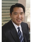
Kevin Masuda Photo 1

Kevin Seichi Masuda, Los Angeles CA - Lawyer

Address:
355 S Grand Ave Ste 3500, Los Angeles, CA 90071
213-6839287 (Office), 213-6834087 (Fax)
Licenses:
California - Active 1992
Education:
University of California - Berkeley
Harvard University Law School
Specialties:
Partnership - 34%
Business - 33%
Mergers / Acquisitions - 33%

Kevin Masuda resumes & CV records

Resumes

Kevin Masuda Photo 19

Operations Specialist

Location:
Los Angeles, CA
Industry:
Internet
Work:
Bird
Operations Specialist
Education:
Arizona State University 2009 - 2013
Bachelors, Bachelor of Arts, Psychology
Maranatha High School 2005 - 2009
Skills:
Customer Service, Microsoft Office, Microsoft Excel, Pos, Communication, Phone Etiquette, Wholesale, Sales, Merchandising, Retail Sales Experience, Retail, Customer Retention, Visual Merchandising, Inventory Management, Time Management, Public Speaking, Business To Business, B2C, Exceeding Targets, Detail Oriented, Teamwork, Operational Planning, Start Ups, Data Analysis, Warehouse Operations, Testing, Technical Support, Data Entry, Tableau, Google Apps, Geographic Information Systems, Json
Interests:
Crossfit Is Life
Traveling
Especially Basketball
Camping
Sports
Amateur Burger Critique
Languages:
Korean
English
Kevin Masuda Photo 20

Kevin Masuda

Location:
Los Angeles, CA
Industry:
Semiconductors
Work:
Rockley Photonics Inc. Feb 2017 - May 2019
Product Development Engineer
Transphorm Inc. Sep 2010 - Mar 2015
Process Engineer
Transphorm Inc. Oct 2009 - Sep 2010
Manufacturing Technician
Education:
University of California, Los Angeles 2004 - 2009
Bachelors, Electrical Engineering
University of California
Skills:
Semiconductors
Kevin Masuda Photo 21

Kevin Masuda

Location:
Los Angeles, CA
Industry:
Hospitality
Work:
Mgm Grand Hotel & Casino Las Vegas Apr 2011 - Jun 2012
Title 31 Compliance Supervisor
Mgm Grand Hotel & Casino Las Vegas Jul 2007 - Mar 2011
Title 31 Compliance Auditor
Bellagio Sep 2005 - Jun 2007
Casino Pit Clerk
Barinco International Corp Jul 2002 - Dec 2004
Import and Export Specialist
Education:
Venice Senior High 1986 - 1988
Skills:
Customs Brokerage, Product Classification, Harmonized Tariff Schedule, Ctrs, Suspicious Activity Reporting, Anti Money Laundering, Cbp, Compliance, Employee Training, Time Management, Import/Export Operations, Bank Secrecy Act, Hospitality, Hiring, Casino Gaming, Resorts, Team Building
Kevin Masuda Photo 22

Partner

Location:
355 south Grand Ave, Los Angeles, CA 90071
Industry:
Law Practice
Work:
Gibson, Dunn & Crutcher Llp
Partner
Munger, Tolles & Olson Llp Apr 1996 - Aug 2017
Partner
Education:
Harvard Law School 1989 - 1992
Doctor of Jurisprudence, Doctorates, Law
University of California, Berkeley 1985 - 1988
Bachelors, Bachelor of Arts, Economics, Business
Skills:
Corporate Law, Intellectual Property, Securities Regulation, Litigation, Commercial Litigation, Entertainment Law, Mergers and Acquisitions, Securities Litigation, Competition Law, Joint Ventures, Negotiation
Kevin Masuda Photo 23

Kevin Masuda

Kevin Masuda Photo 24

Kevin Masuda

Kevin Masuda Photo 25

Kevin Masuda

Location:
United States
Kevin Masuda Photo 26

Kevin Masuda - Santa Maria, CA

Work:
Transphorm USA Oct 2013 to 2000
Process Development Engineer
Transphorm USA Oct 2010 to Oct 2013
Process and Sustaining Engineer
Transphorm USA Oct 2009 to Oct 2010
Production Technician
Education:
University of California at Los Angeles - Los Angeles, CA 2009
Bachelor of Science in Electrical Engineering

Publications & IP owners

Us Patents

Polarization Splitter-Rotator Having Silicon Based Waveguide With Silicon Nitride Segment

US Patent:
2022019, Jun 23, 2022
Filed:
Jul 12, 2021
Appl. No.:
17/372988
Inventors:
- Mountain View CA, US
Kevin Masuda - Alhambra CA, US
Brett E. Huff - Keller TX, US
Pradeep Srinivasan - Fremont CA, US
International Classification:
G01S 7/499
G02B 27/28
G02B 6/126
G01S 17/06
G02B 6/122
Abstract:
A polarization splitter-rotator (PSR) is described. The PSR having a silicon nitride based waveguide to split and rotate an optical beam. The silicon nitride based waveguide having a first silicon nitride segment including a first layer and a second layer coupled with the first layer.

Distributed Feedback Laser

US Patent:
2020030, Sep 24, 2020
Filed:
Mar 20, 2020
Appl. No.:
16/826122
Inventors:
- London, GB
Kevin Masuda - Alhambra CA, US
Pradeep Srinivasan - Fremont CA, US
International Classification:
H01S 3/067
G02B 6/12
Abstract:
A Distributed Feedback Laser (DFB) mounted on a Silicon Photonic Integrated Circuit (Si PIC), the DFB having a longitudinal length which extends from a first end of the DFB laser to a second end of the DFB laser, the DFB laser comprising: an epi stack, the epi stack comprising: one or more active material layers; a layer comprising a partial grating, the partial grating extending from the second end of the DFB laser, only partially along the longitudinal length of the DFB laser such that it does not extend to the first end of the DFB laser; a highly reflective medium located at the first end of the DFB laser; and a back facet located at the second end of the DFB laser.

Optoelectronic Component

US Patent:
2017029, Oct 19, 2017
Filed:
Nov 10, 2016
Appl. No.:
15/321723
Inventors:
- London, GB
Hooman ABEDIASL - Los Angeles CA, US
Damiana LEROSE - Pasadena CA, US
Kevin MASUDA - Alhambra CA, US
Andrea TRITA - Pasadena CA, US
Aaron ZILKIE - Pasadena CA, US
International Classification:
G02F 1/025
G02F 1/21
G02B 6/122
G02B 6/136
G02B 6/13
G02F 1/17
G02B 6/12
G02F 1/21
Abstract:
An optoelectronic component including a waveguide, the waveguide comprising an optically active region (OAR), the OAR having an upper and a lower surface; a lower doped region, wherein the lower doped region is located at and/or adjacent to at least a portion of a lower surface of the OAR, and extends laterally outwards from the OAR in a first direction; an upper doped region, wherein the upper doped region is located at and/or adjacent to at least a portion of an upper surface of the OAR, and extends laterally outwards from the OAR in a second direction; and an intrinsic region located between the lower doped region and the upper doped region.

NOTICE: You may not use BackgroundCheck or the information it provides to make decisions about employment, credit, housing or any other purpose that would require Fair Credit Reporting Act (FCRA) compliance. BackgroundCheck is not a Consumer Reporting Agency (CRA) as defined by the FCRA and does not provide consumer reports.